The three stories logged on this beat point to a single structural shift in the semiconductor industry: chipmakers are abandoning the idea that one general-purpose processor can serve every AI workload. Instead they are splitting silicon into narrower product lines, finer-grained dies, and in one case an entirely new interconnect layer to hold those dies together. The through-line is specialization, and the connective tissue is the chiplet.
AMD Splits One Server Line in Two
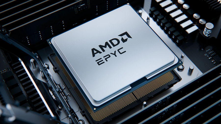
The clearest expression of the trend comes from Advanced Micro Devices, which today introduced the Epyc 6 series for server CPUs, also known as Venice. As SiliconANGLE reported, the line comprises 10 CPUs organized into two distinct groups. One set pairs a large number of relatively slow cores with the other set's fewer, higher-frequency cores, and the two groups are aimed at different jobs within the same generation of product.
That is a meaningful departure from how server CPUs have historically been sold. A single Epyc family with a broad core count was previously expected to cover web serving, database work, and emerging compute alike. AMD's stated framing is AI agent workloads, which is the tell. Agentic software tends to run in bursts: long stretches of orchestration and tool calls that reward many threads at modest clock speeds, punctuated by reasoning steps that reward fewer, faster cores. Rather than force customers to buy one compromise part, AMD is selling them a menu. For US cloud operators and enterprises building agent infrastructure, that means CPU selection becomes a workload-matching exercise rather than a straightforward generational upgrade.
Google Widens the TPU Portfolio
Google is making the same move on the accelerator side. As TechCrunch reported, the company broadened its AI hardware portfolio with two new specialized tensor processing units, extending its chip lineup to use cases including confidential model training and configurations with more memory capacity. The significance is not the number of chips but the direction of travel: Google is no longer treating the TPU as a single product family with successive versions, but as a portfolio segmented by workload requirement.
Confidential training is a distinct demand from raw throughput. It implies a customer willing to trade peak performance for isolation, and it implies silicon designed around that trade rather than around a benchmark. The memory-capacity variant points the same way, since memory capacity is the binding constraint for large models and is not something a faster compute die can fix. Both moves matter to the US market specifically because Google's TPUs underwrite a large share of domestic AI capacity, and segmentation there raises the bar for merchant silicon vendors selling into the same customers.
The Chiplet Becomes the Unit of Design
The common thread in both product moves is that neither is achievable with a single monolithic die. Splitting a server CPU family into core-heavy and frequency-heavy variants, or building accelerators that differ mainly in memory capacity and isolation, is far cheaper when the processor is assembled from separate silicon dies than when it is printed as one piece. Segmentation at the product level is enabled by disaggregation at the manufacturing level.
That makes the third story the enabling one. Staera Semiconductor Inc. launched today with $4.6 million in pre-seed funding to develop an optical interconnect for chiplets, as SiliconANGLE reported. Openspace Capital, a Singaporean fund, led the investment, joined by SGInnovate, Black Kite Capital, 28 Holdings, In Group and financial software company Decimus Technologies. Staera's premise, per the report, is that high-end AI accelerators comprise multiple chiplets, and that linking those dies is becoming the limiting problem.